Uncut Gem
The World's first fully open-source, hackable quantum sensor!
Brought to you by Quantum Village Inc., a 501(c)(3) Quantum Technology Company.
Uncut Gem
A prototype Full Stack fully Open Source NV Center Diamond Magnetometer.
V1 - this document and repository.
V2 - COMING SUMMER 2025!
There are several sections detailing the parts of the build - please use the quick links on the side to take you to the relevant sections.
The GitHub repository for this project may be found at: https://github.com/QuantumVillage/UncutGem

Project Mission
We are creating the world's first fully open-source quantum sensing platform designed from the start to be accessible, future-proof, and most importantly; hackable!
We are designing, building, provisioning, and aiming for distribution of a fully open hardware platform, complete with fully open firmware, that gives a firm basis for anyone to start learning about quantum sensing through nitrogen vacancy center diamond magnetometry.
By incorporating key design decisions, we are building the basis for what we think will be quantum technology's 'Apple II moment'; the opportunity for anyone who is curious to gain access to a quantum device that they can operate safely at home, with the full capability to customize, improve, develop with, and share knowledge about this incredible technology.
Keep me up to date!
If you'd like to be kept up to date with developments, releases, and pre-order notifications - sign up here:
Design Philosophy
We have used the following four principles to guide the initial development of this project:
- Aim to create a platform for exploration.
- Use Consumer Off-the-shelf (COTS) components as much as possible.
- Create a hardware stack that allows as many aspects of the sensing process to be ‘software problems’ as possible.
- Where assembly is required, simplify!
Features
The design is in two iterations, but generally our features are:
- Using easy-to-acquire, all-generic parts for our PCBs.
- Low-noise photodiode signal amplifier design that is robust and inexpensive.
- Using off the shelf, low cost, widely available daughter boards.
- Easy and reasonably compact construction from carefully considered design.
- Optimized control stack and firmware, written using Arduino IDE for portability and future-proofing.
- Full build guide and growing documentation.
- Growing community around these devices.
Contents Overview
We aim to cover all of the essential information for someone interested to learn about quantum sensing with Nitrogen Vacancy Centre Diamonds, and then have the information and parts-list to go ahead and construct such a device. To that end, we cover:
- The basic science behind this kind of solid state quantum sensing
- A run down of our design choices and devices/parts used to make the sensor
- A build guide for putting together a working sensor
Everything is open source, including the firmware, and we welcome contributions to improve this design!
Why Open Source?
“Information flow is what the Internet is about. Information sharing is power. If you don't share your ideas, smart people can't do anything about them, and you'll remain anonymous and powerless.” -- Vint Cerf
We think that more projects in quantum technology should be open source, so that quantum tech can benefit from the rich ecosystem of 'ready-made' tooling that our existing software and classical technology stacks have enjoyed! We firmly believe that by creating an open-source baseline for quantum and quantum-related technologies we immediately gain a number of things:
- The dissemination of knowledge around quantum technologies allows the general workforce to gain the skills needed to further develop quantum tech.
- By creating a testbed platform that is designed to be hackable, it is natural to extend its functionality into areas that nobody is currently considering.
- By using COTS parts and creating and open design, we can drive down the costs associated with quantum sensing.
- The value proposition for commercial products and services is immediate by comparison to an open-source 'free' baseline.
The Science of Nitrogen-Vacancy Diamond Magnetometry
The following articles are particularly useful for understanding the physics of what is going on:
- Stegemann et al. - Modular low-cost 3D printed setup for experiments with NV centers in diamond - https://iopscience.iop.org/article/10.1088/1361-6404/acbe7c
- Acosta and Hemmer - Nitrogen-vacancy centers: Physics and applications - https://link.springer.com/article/10.1557/mrs.2013.18
- Frellsen and Ahmadi - Sensing magnetic fields with diamonds and green laser light - https://quantum-journal.org/views/qv-2018-07-17-10/
Copies are in the ./resources folder.
Diamond Mounting
This document captures the information surrounding the development of the diamond mount.
Core Components
There are 5 main components:
- The Diamond itself
- The epoxy block containing it
- The aerial wire for the microwave signal
- The photodiode placement
- The red gel light filter.
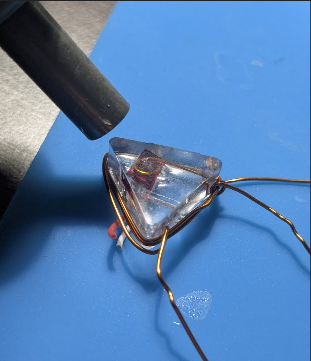
The 'Secret' Behind the Build
The open secret in this build is to essentially use parts that are designed for jewellery making. The silicone moulds, UV epoxy, and use of 24AWG copper wire are all common components in craft jewellery making - the kind found on Etsy or similar. So if you cannot acquire precisely the parts we list here, then you can always search for substitutes that are used in this production style.
The Diamond
The diamond is ~750um in size - essentially a large grain of salt/small grain of sand in size. It is a purple-ish colour, brought on by the presence of the N-vacancy centers. The important thing to remember is that this is an inert rock that can convert green light @ ~520nm into red light @ ~620nm in the presence of several bands of microwave frequencies. These may be acquired but only in bulk from companies like Element Six and Adamas Nano.
Epoxy block containing it
The epoxy that we have eventually worked out is best is UV cured clear epoxy. Clear epoxy has reasonably good optical properties, and UV cured epoxy (e.g. of this kind on Amazon.co.uk) is widely available. We make use of UV cured epoxy for fast iteration and prototyping. Whilst slower setting epoxies may have slightly nicer chemical properties for other applications, the use of very stable materials (diamond, copper, plastic film) means that faster setting epoxy is perfectly fine to use.
The epoxy is best moulded in silicone moulds - we used some of the smaller slightly thicker shaped moulds from a 'epoxy jewellery mould kit' we found on Amazon (sadly no longer available). There are also useful mould sizes advertised for use in making sweets/confectionery or for moulding small chocolates. All of the ones that are useful are usually in the size range of 10-20mm.
Aerial wire for the microwave signal
24AWG enameled copper wire is used for two things in this build - structural holding of the epoxy block, and delivering the microwave signal. The signal aerial has to have a small loop formed in the end, and this is placed around the diamond during the layering. This delivers the best signal - we have tried many designs from simple junctions to more adventurous designs, but this was by far uniformly the best design we found!
Photodiode placement
Instead of using optics (mirrors, beam splitters, etc) we place the photodiode, a BPW34 photodiode that we purchased on eBay, directly below the diamond and very close to it. This is because the BPW34 has a relatively large detection surface of 3x3mm. This means that if it is close enough, it will acquire most of the light emitted by one side of the diamond. The BPW is epoxy mounted directly below the diamond for this purpose.
Red gel light filter
There is evidence in PAPER LINK that a red-gel filter, the kind used in theatre or photographic lighting, is 'mostly' as effective as professional grade dichroic mirrors (which let one light band pass through and reflect the rest). As such, we were able to place this layer interstitially between the diamond and covering the photodiode detection surface completely. In experimenting we found that only 1 layer was needed in order to acquire meaningful signal.
Construction
We do this in three epoxy pours, which we'll describe in turn. The diagrams are purely illustrative, and are not drawn to scale.
Layer 1
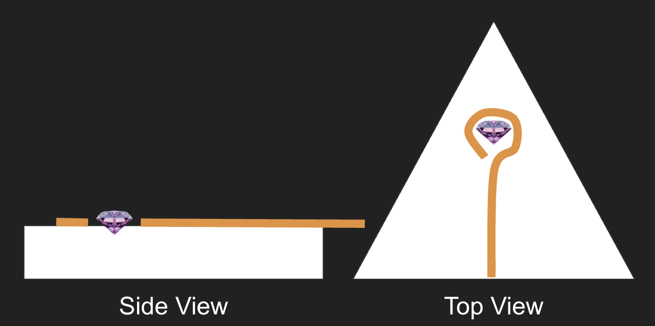
First lay down a layer of epoxy and proceed to harden it. Once done, carefully place the diamond in the middle of the antenna loop on top of this layer.
Layer 2
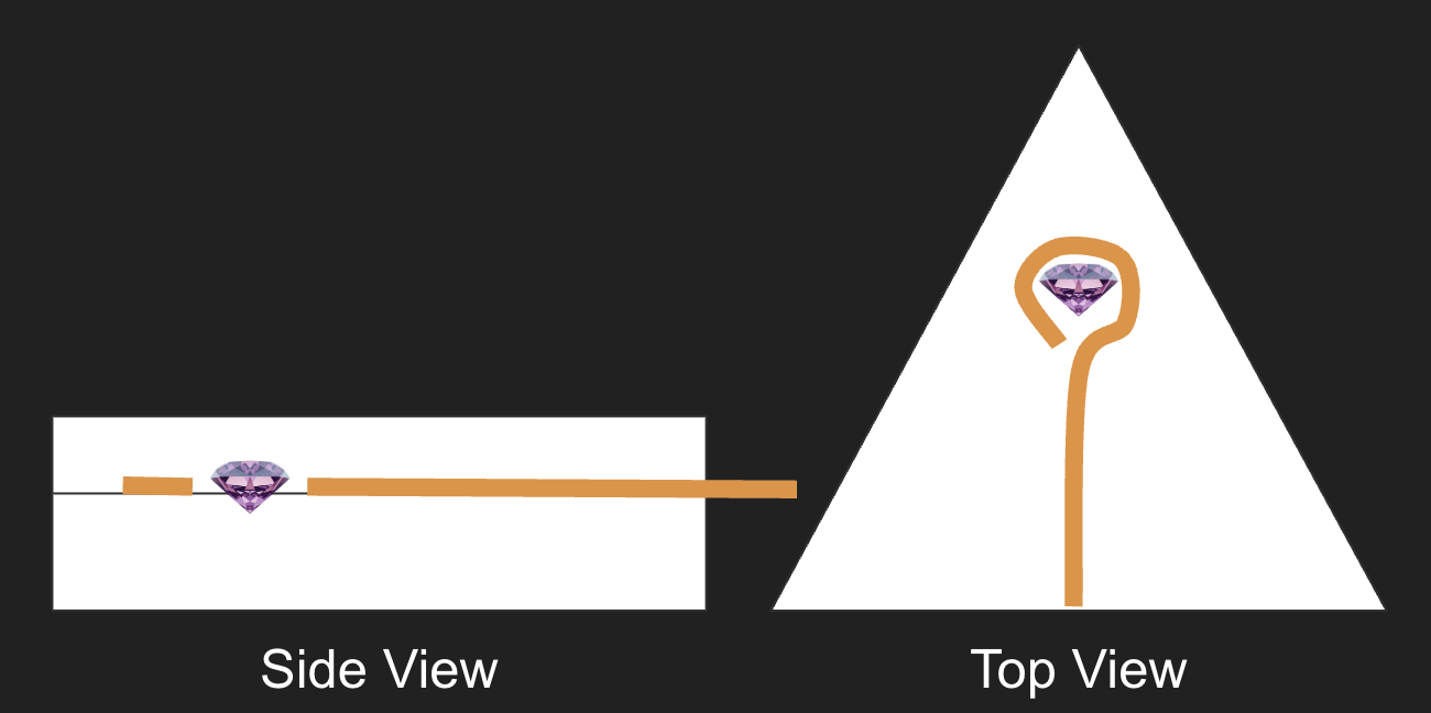
Once the diamond and antenna are in place, proceed to pour another layer of epoxy over the top. We use toothpicks to maneuver things into just the right positions before hardening again.
Layer 3
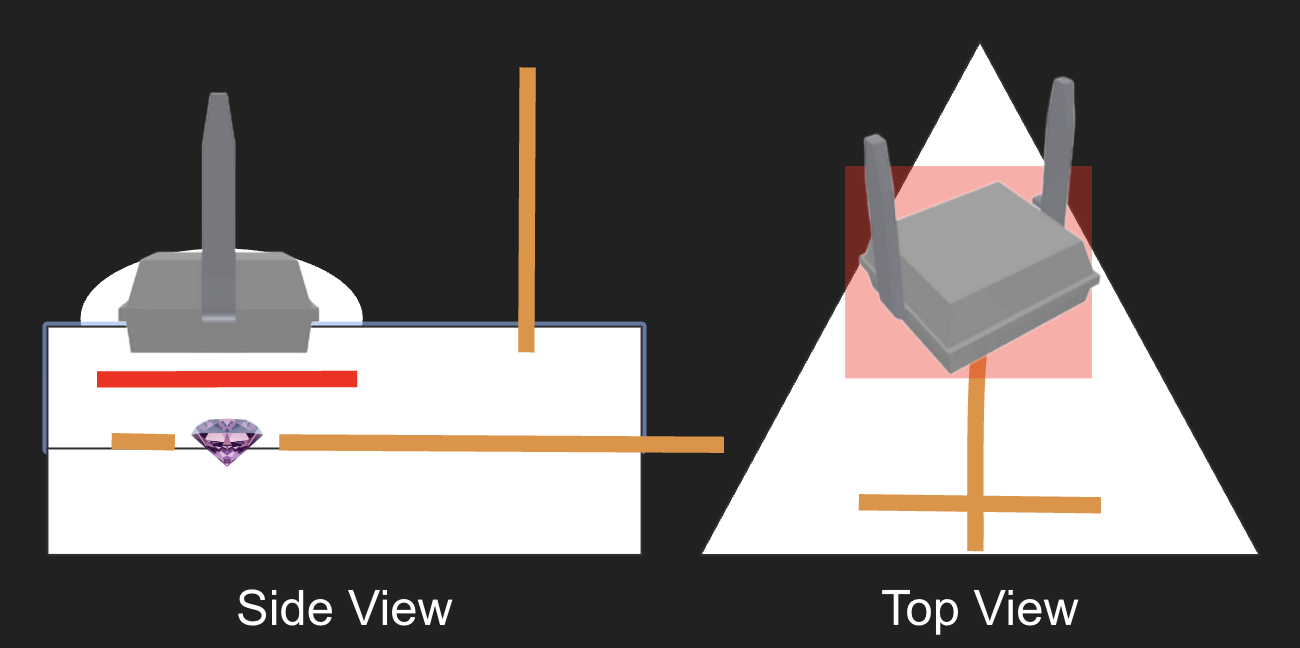
With the diamond now set, we carefully place a 5x5mm square of red filter over the diamond. The photodiode should then be placed directly over the diamond, with the diamond central to the sensor area.
Once this is done, we then pour the rest of the epoxy and place any copper supports or mechanical fixings into this layer, before hardening.
Often, we reinforce the photodiode with an extra blob of epoxy around it to make sure it is immovable.
Decapsulating the Diamond
Should you need to fix an error, whilst the photodiode, red filter, and copper wire may be very hard to retrieve from the epoxy, the diamond is very easy to retrieve; many epoxies (such as the one above) soften at around 200C, so we simply use a small hot air device to heat the epoxy prism until it is soft, and then use pointed tweezers to retrieve the diamond.
This method is relatively mess-free and quite safe. We have yet to damage a diamond in this process. The other components are more hit-and-miss as to whether they can be retrieved this way.
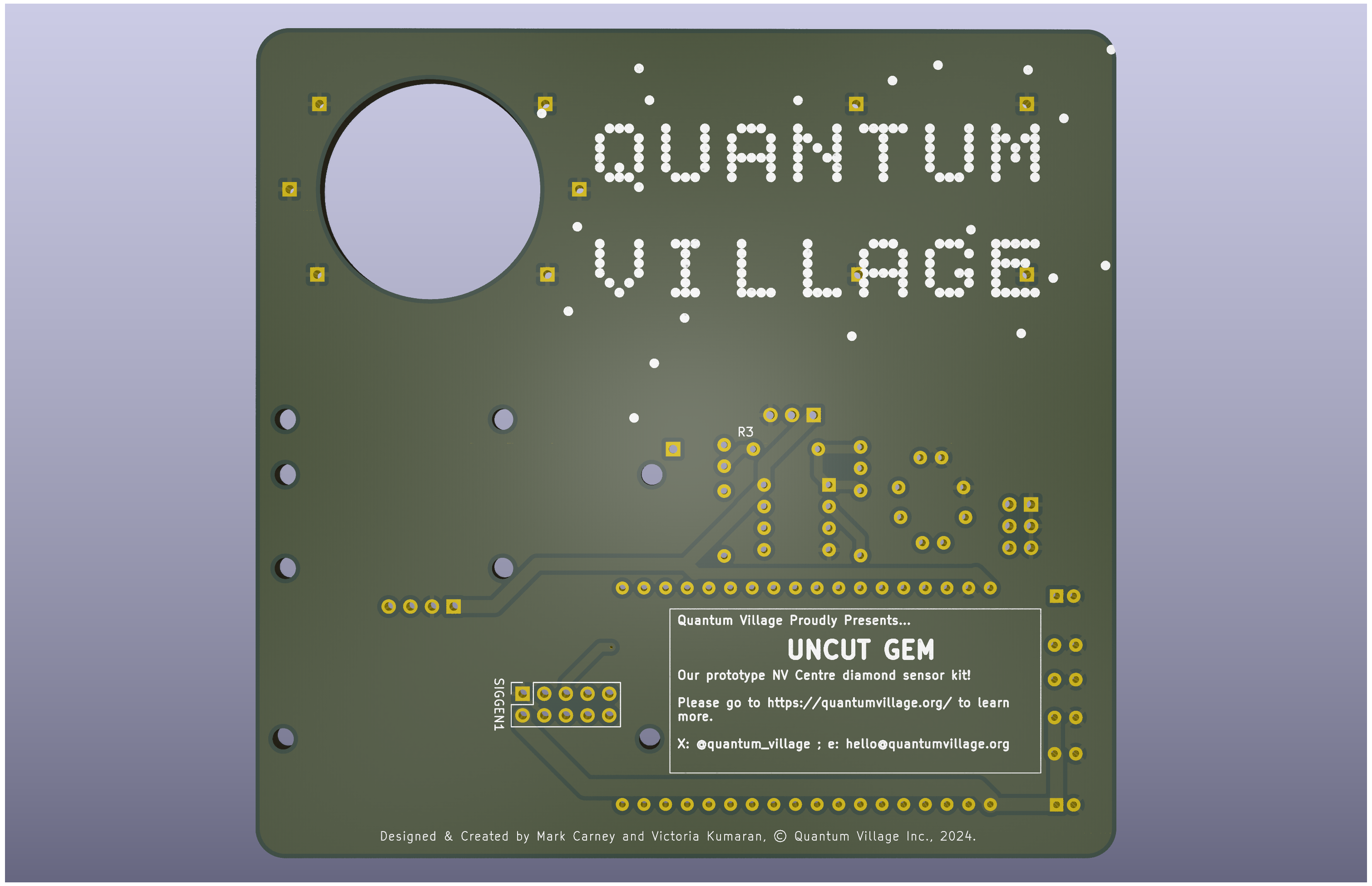
PCB
This folder contains the entire KiCad project for the diamond sensor, with full electronics. The Git History contains previous versions, including the version first presented at BSides London in Dec 2024!
The schematic may be found here.
Here are two renders of the first version of the board:
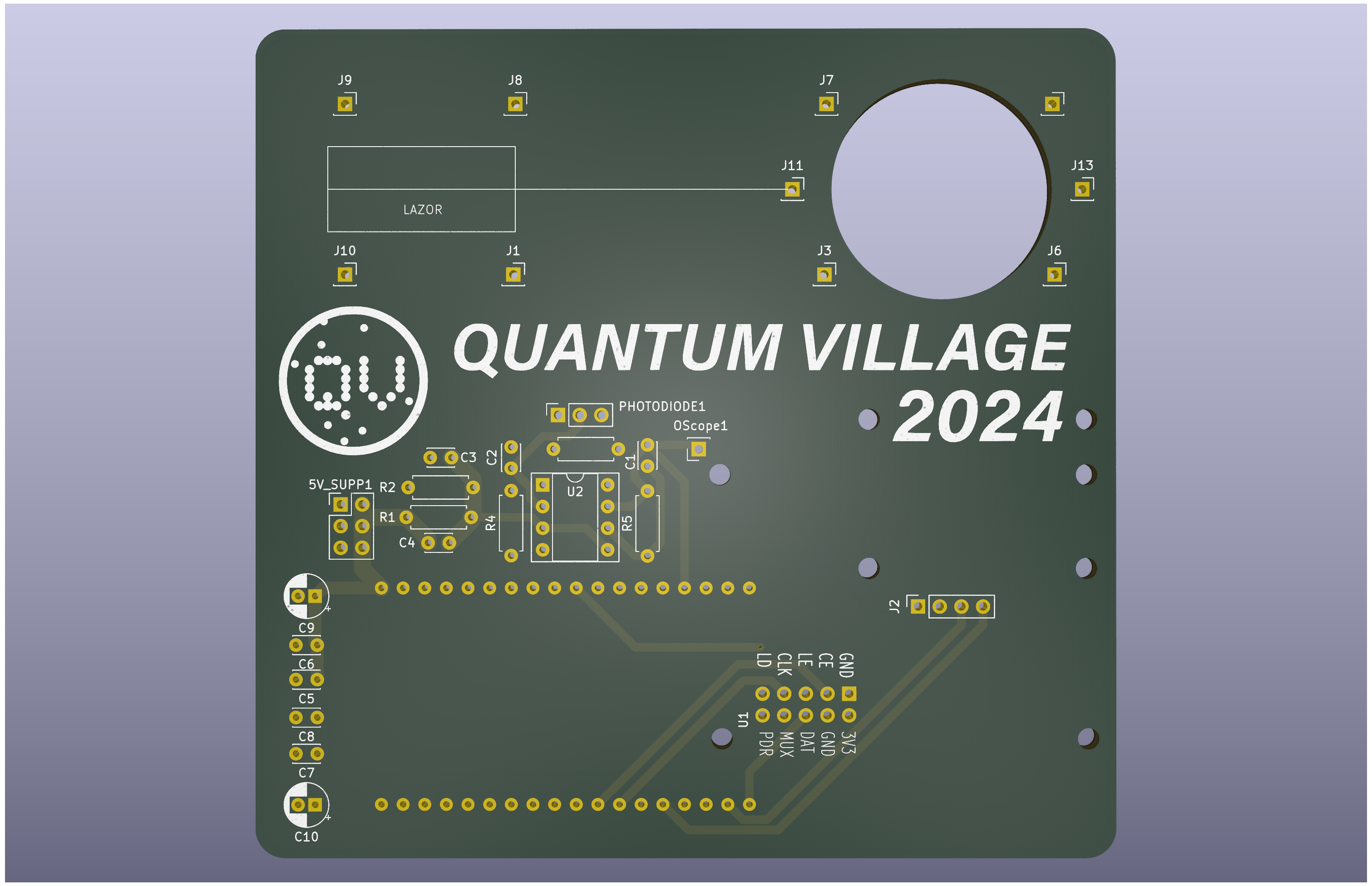
Bill of Materials
Here is a bill of materials for the various parts and connections on the board:
| Reference | Part Value | Qty |
|---|---|---|
| 5V_SUPP1 | Conn_02x03 | 1 |
| C1 | 104 | 1 |
| C2 | 33 | 1 |
| C3,C4,C5,C6,C7,C8 | 100nF | 6 |
| C9,C10 | 10uF | 2 |
| J2 | OLED Screen Interface | 1 |
| OScope1 | OScope | 1 |
| PHOTODIODE1 | Conn_01x03_Socket | 1 |
| R1,R2,R3 | 1k | 3 |
| R4 | 1M | 1 |
| R5 | 47k | 1 |
| SIGGEN1 | Conn_02x05 | 1 |
| U1 | DOIT-ESP32-DEVKIT-V1 | 1 |
| U2 | TL082 | 1 |
NB - Here are some notes about this design:
- Capacitors C5-10 are optional, mostly included to deal with unsteady USB power supplies.
- Capacitors C1 and C2 turn the transimpedence amplifier into integrator mode. If they are omitted, it will operate as a regular inverting OpAmp.
Additional COTS Parts
There are several additional parts that are needed for this pariticular version, detailed below.
ADF4351 Dev Board
The specific board used is this part on AliExpress. The key part is to expose the SPI pins (DAT, CLK, CE) as well as the power/ground and LE (Load Enable) pin.
40db Gain RF Amplifier for 30-4000MHz
Specifically this part on Aliexpress. This just requires power and ground, which are routed to the 5V power and ground connector.
Green Laser Module
We used a module we acquired off Amazon UK (no longer available), but in reality any laser module may be used, as long as it uses provides the following:
- 520nm - 532nm green light
- a laser point of light
- is around 10mm wide by 22mm long.
ESP32 Dev Board
We use one that is 2x rows of 19 pins with the pin-out described in the schematic. You can use 15-pin boards, but you'll have to add wires for power and ground manually.
1.3" OLED Screen
These are standard OLED boards using SH110X-based screens driven by I2C (not SPI). BEWARE - many of the screens swap VDD and GND. This design uses a board with pins in order (as you look at the screen): VDD/GND/SCK/SDA
If your screen has GND/VDD/SCK/SDA, then you need to do some work on the PCB to fix it, or acquire a different screen.
Cost per Device
The ballpark costs are as follows (in GBP):
| Item | Number | Cost |
|---|---|---|
| Battery pack | 1 | Free to £5 |
| OpAmp + electronics | 1 | up to £5 |
| Laser Module | 1 | ~£5-15 |
| ADF4350/1 MW Generator | 1 | £15-25 |
| MW Gain (40dB) + BNC | 1 | £10 |
| PCB (unit from run) | 1 | ~£5 |
| OLED Screen | 1 | £5 |
| ESP32 board | 1 | ~£10 |
| NV Center Diamond | 1 | ~£10 |
| Epoxy and Cu Wire | 1 ea. | £10-15 |
| TOTAL | ~£115 |
Firmware
An ESP32 development board is used as both controller for the ADF4351 signal generator and as an Analogue-to-Digital Converter (ADC) to read the signal from the photodiode amplifier.
The firmware is included in the src directory.
The ADF4351
The ADF4351 is the key component in this design - here are some key resources for debugging and developing out more functionality using it:
- The ADF4351 Cheatsheet - Analogue Devices - https://www.sv1afn.com/images/usrImage/1-12-2019-21-38-5de432db94746.pdf
- The ADF4351 Datasheet - https://www.analog.com/media/en/technical-documentation/data-sheets/adf4351.pdf
Copies are also provided in the /resources folder.
The ADF4351 is a PLL frequency generator chip designed for generating 35MHz to 4.4GHz signals. Primarily designed for use in wireless transmission hardware and protocols, we are using here as our main software controllable source of microwaves.
The ADF4351 accepts signals over an SPI-based protocol, for which we use the built-in Arduino IDE functions with some additional code to take care of the Latch Enable (LE) pin setting.
Overview of Key Functions
The firmware has a number of key files:
uncut-gem.inois the main sourcefile for Arduino IDE- This contains the
setup()andloop()functions defaults. - This file sets up all of the devices, then enters a function loop.
- This contains the
sweep_array.hcontains pre-calculated frequency values to send to the ADF4351.ADF4351.cppandADF4351.hare adapted versions of code from Analog Devices. They do not run as they usually would as that was far too noisy.
The control flow looks something like this at a high level, beginning from setup():
flowchart TD
    n1(["setup()"]) --> n8["Calibration Routine"]
    n8 --> n7
    n2["Set next Frequency"] --> n3["Take average of 10 meausrements"]
    n3 --> n4["Draw average to screen"]
    n4 --> n5["Loop Done?"]
    n5 -- Yes --> n6["Calculate & draw cumulative average to screen"]
    n7["Enter Microwave Sweep Loop"] --> n2
    n5 -- No --> n2
    n6 -- Loop! --> n7


    n2@{ shape: rounded}
    n3@{ shape: rounded}
    n4@{ shape: rounded}
    n5@{ shape: diam}
    n6@{ shape: rounded}
    n7@{ shape: rounded}
    n8@{ shape: rounded}
    style n1 stroke-width:4px,stroke-dasharray: 0
Some Considerations in Firmware
There were many considerations made to improve the accessibility and reliability of the sensor's operation.
Arduino IDE
The Arduino IDE is a very forgiving generic development environment for microcontrollers. It is aimed primarily at hobbyists, but has gained traction as a very easy way to 'fast prototype' microcontroller application designs.
We make use of it in this project so that as many people as possible can make use of the code on as many platforms as necessary. Rather than writing specific SPI handling code for the ADF4351, we instead can just make calls to spi->transfer(data[i]); from a generic SPI code API that is then ported to devices individually. Although there are many things in this code that are specifically coded for the ESP32 (such as pin definitions) these are all easily changeable to make the code work on other microcontrollers, based on availability.
Hard Coding ADF4351 Freq Values
The PLL (Phase-Locked Loop) interface on the ADF4351 derives its output frequency from several settings, each of which as to be calculated carefully before sending to the device.
However, calculating these values on the fly from a given frequency input has two major drawbacks:
- Time - the computation can be slow, especially on older microcontrollers.
- Noise - calculating the correct values can generate more noise from the microcontroller during operation.
Regarding time, the reason things slow down is due to the fact that some microcontrollers have to do a lot of work to parse large numbers (in the billions for GHz). So pre-computing saves a lot of time, at the expense of a relatively small amount of memory - ~30bytes for each frequency.
Regarding noise - the measurements we are looking for are very small, so a lot of amplification is in place to find them. If the microcontroller's power draw is screaming in the background, then it results in a very messy signal. However loading bytes in/out of memory and out over SPI is relatively quiet. As such, rather than doing side-channel amplification on our microcontroller, we instead can get at the signal from the diamond.
UNCUT GEM - Build Guide
This is as comprehensive build guide as we can make for the UNCUT GEMS open source NV center diamond sensor!
Things we don't cover:
- How to solder - lots of help out there for that!
- How to have a PCB manufactured - but we do provide files that should be compatible with most manufacturers, e.g. JLCPCB, PCBWay, etc.
- For this step, zipping up the contents of the PCB
Prod_filesfolder should be enough.
Preparing the Epoxy Diamond Mount
This is thoroughly covered in the section about the hardware, so we'll refer you to that for now. Once you have created your own quantum diamond prism, you can continue from here.
Note on USB Power
We recommend using an isolated or protected USB supply for testing and operation. Not all computer/laptop USB power circuits are built to handle the occasional faults that may occur, and you may well damage your equipment, as well as the sensor, if care it not undertaken.
Populating the PCB
Assuming you have a PCB, we recommend the following steps:
- We first recommend soldering the components for the transimpedence amplifier:
- First, solder the TL082 dual opamp chip - use a DIP chip socket, or solder directly if you know what you are doing.
- Next, solder the resistors and capacitors, only adding C1 and C2 if you want to use the opamp as an integrator.
- Trim the leads on the back.
- Solder the sockets for the ESP32 dev board, the OLED screen, and the 5V/GND supply 3x2 pin socket block.
- Next, solder the 5x2 pin socket for the ADF4351 board
- Note - this socket is soldered on the back of the board. So you solder on what is the front of the board.
- Before placing the boards, bolt in place some appropriately long brass PCB mounts.
- First, plug in the ESP32 and power up:
- Check that a steady 5V is coming from the 5V supply socket
- 3.3V from the socket for the ADF4351 board.
- Check that the legs of R1 and R2 have the correct voltage divider voltages; 5V, 2.5V, and 0V.
- If any of these aren't correct, check for shorts!
- Compile and upload the firmware to the ESP32.
- With this successful, mount the ADF4351 to the back, and the RF amplifier board to the front of the PCB.
- The mounting for these overlap but are on different sides of the board.
- The silkscreen on the front of the PCB should match the pin definitions on your development board.
- Connect the ADF4351 and RF amplifier with a standard, short length, socket SMA to socket SMA cable.
- Test the board so far:
- Apply a short antenna to the free side of the RF amplifier (if available).
- Power up the board and check that the
LOCKLED lights up. - If this is fine, then check the frequency is as described in the firmware mode you have selected.
- Most of the hardcoded modes centre around 2880MHz.
- Plug in the laser module to the 5V/GND socket paying close attention to polarity!
- Plug in the photodiode connector from the assembled diamond holding prism.
- Connect the microwave antenna to the RF amplifier output.
- If you have crimped an SMA connector, then you can just screw this onto the mounted connector on the RF amplifier board.
- If you have not, then you may carefully solder the antenna wire to the output pin of the same connector.
- Carefully inspect the soldering joint to ensure no short circuits have been introduced.
- At this point TRIPLE CHECK FOR ELECTRICAL SHORTS before powering on! At this point, an unintended short can damage all three of the daughter boards.
- Plug in the OLED screen board and power up - if the text
Calibrating...is shown, then the device is working!
If the board powers on find after all this, and all checks are passed, then you should proceed to aligning!
Aligning the Laser and Diamond
The simplest way is to mount the lasers on some enameled copper wire, and use the structural properties therein to hold the laser and epoxy prism in place.
NB - you MUST use enameled copper wire, else you will create shorts that will definitely damage your device and any device it is connected to!
When aligning, use Red laser goggles or a sample of red filter gel to align the laser such that the diamond is shining very brightly with red light!
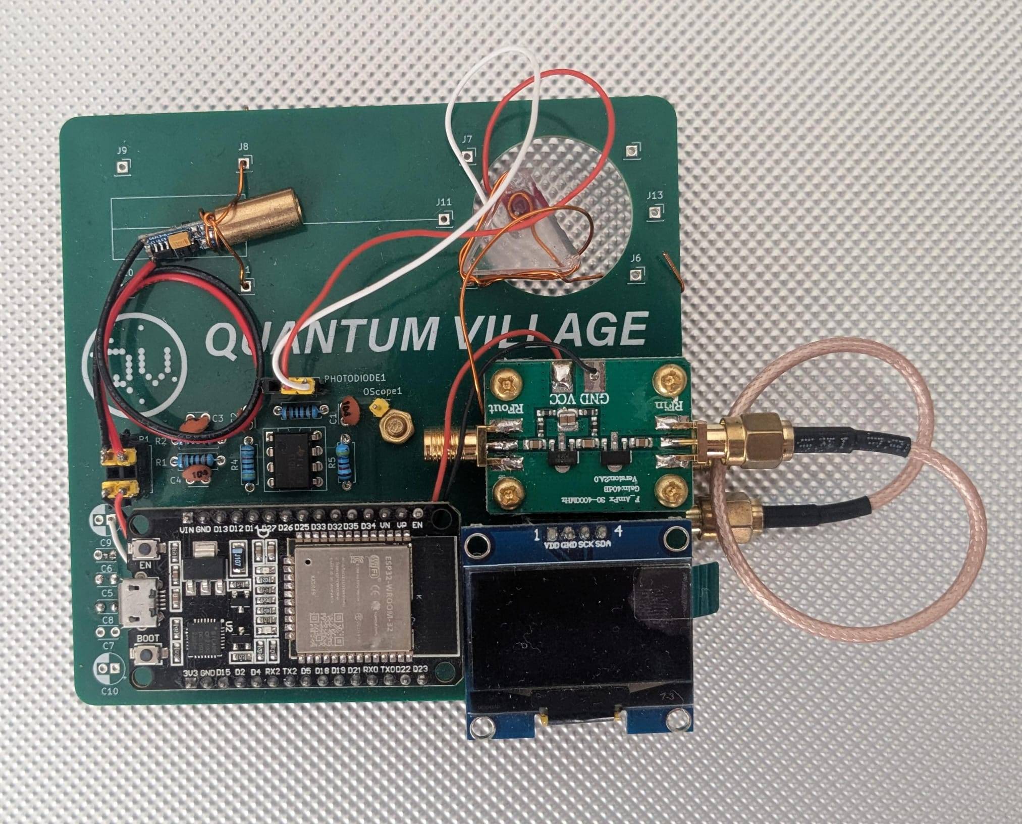
Completed Board
The finished assembled board should look like this:
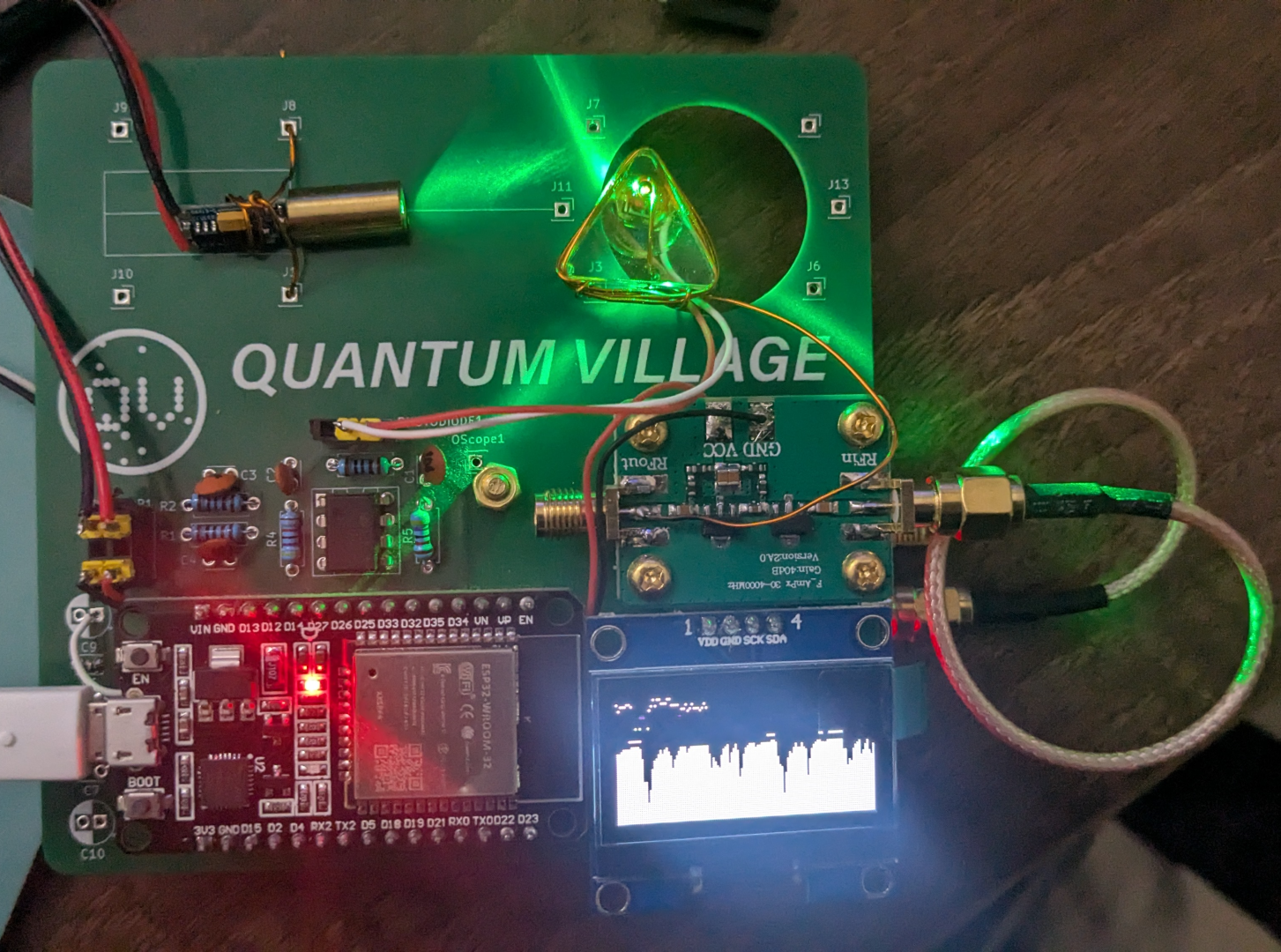
Testing and Operation
To test the magnetometery we recommend the following initial 'signs of life' test:
- Turn off as many environmental/ambient lights as possible.
- Power the device and check that the lower half of the screen is showing a pattern.
- If not, connect to the serial port and check there is data coming from the device.
- Move a small magnet near the diamond and check it registers.
- To confirm the magnet is causing the change, place a small cutout of paper over the top of the prism (to block light changes) and repeat moving a magnet close.
If all this has been successful - CONGRATULATIONS!!
Acknowledgements
We would like to thank the following folk for their help during this project:
- Victoria Kumaran - Prototyping, design and conceptualisation, and project contextualisation.
- Dr. Mark Carney - Prototyping, initial designs for hardware/firmware.
- Dr. Matthew Markham - Key contact at Element6, tech support and providing quantum material.
- Rick Altherr - Design and engineering expertise and support.
- David Bengtson - RF expertise and electronics support.
- Prof. Ben Varcoe - testing support and physics expertise/advisory.
- Dr. Brian McDermott - Expert Advisor.
- Elle Dowling - Orthographic Services.
Resources
Here are some key resources for this project:
- ADF4351 Datasheet
- ADF435x Cheatsheet
- Stegemann et al. - Modular low-cost 3D printed setup for experiments with NV centers in diamond - Stegemann_2023_Eur._J._Phys._44_035402.pdf
- Acosta and Hemmer - Nitrogen-vacancy centers: Physics and applications - mrs.2013.18.pdf
- Frellsen and Ahmadi - Sensing magnetic fields with diamonds and green laser light - Sensing%20magnetic%20fields%20with%20diamonds%20and%20green%20laser%20light%20–%20Quantum.pdf)